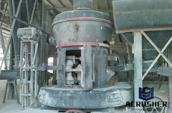
silicon wafer backgrinding process
Warping of silicon wafers subjected to backgrinding process. This study investigates warping of silicon wafers in ultraprecision grindingbased backthinning process.

 WhatsApp)
Warping of silicon wafers subjected to backgrinding process. This study investigates warping of silicon wafers in ultraprecision grindingbased backthinning process.
One is slicing the silicon ingot, the other is wafer back grinding after circuit process is completed. ... How thin can we cut silicon wafers? Update Cancel.
Because the thinning of the whole wafer at the back ... use a twostep process including a coarse grinding ... Wafer Thinning: Techniques for Ultrathin Wafers ...
Figure 1. a) A backgrinding process leaves a characteristic scratch pattern on the back of the wafer. b) The back of the die from certain locations on the wafer have ...
parallelism between the front and the back surface. Secondly, the grinding ... achieve this we need to understand thoroughly the process of semiconductor wafer grinding
Plasma systems for wafer stress relief ... process containing no free ions or electrons that could potentially charge the surface of the wafer. The backgrinding ...
This paper presents the effect of back grinding on the mechanical properties of the active side of the multilayered lowk stacked die. Lowk stacked wafers
... which ensures against wafer surface damage during backgrinding and prevent wafer ... The wafers are also washed with deionized water throughout the process, ...
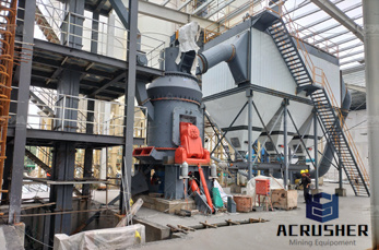
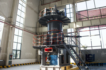
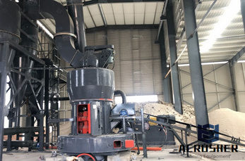
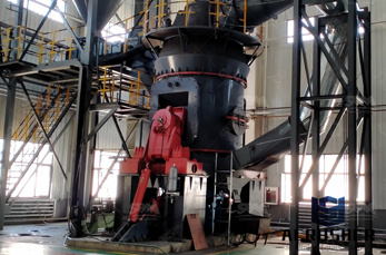
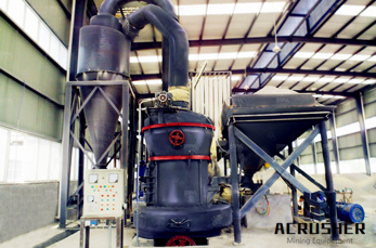
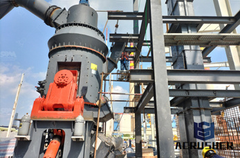
wafer back grinding process Products for Back Grinding Process This is an advanced back grinding tape laminator for thin wafers that achieves tensionfree lamination ...
Warping of silicon wafers subjected to backgrinding process. This study investigates warping of silicon wafers in ultraprecision grindingbased backthinning process.
Wafer Back Grinding Tapes; ... Rework Process; White Papers ... Wafers requiring grinding and thinning to 50 microns needs high performance adhesion and yet easily ...
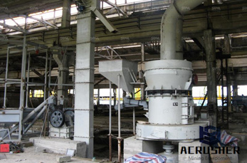
World leading Technology for grinding/thinning of wafer ... fine grinding of prime wafers or back ... grinding process efficiency. Prime wafer ...
Leadingedge Tape B!_ (B Equipment solution created with semiconductorrelated products ''Adwill.'' Fully and semiautomatic wafer mounters for the dicing process.
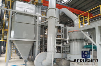
Home / Products / Grinding Process Wafers. ... Back Grinding For Bare Device Patterned Wafers,SVM,Inc. Back grinding is a process that removes silicon from the back ...
The TAIKO process is the name of a wafer back grinding process that uses a new grinding method developed by DISCO This method is different to conventional back ...
This is an advanced back grinding tape laminator for thin wafers that achieves tensionfree lamination. The lineup consists of two product types that vary in ...
Syagrus Systems thin wafer backgrinding and silicon wafer thinning services meets ... more about our Wafer Dicing Process. ... your next back grinding wafer ...
Backend processing refers to assembly and final testing. For use in the back grinding process to polish the backside of the wafer, ACCRETECHTOKYO SEIMITSU ...
Semiconductor Wafer Edge Analysis/4 Stricter requirements in the wafer manufacturing process have made edge measurements important for both 200 mm and 300 mm wafers.
Effects of back grinding process ... Wafer Reclaim and processing services including wafer grinding and thinning, wafer edge trimming, wafer dicing, ...
Wafer Backgrind is the process of grinding the backside of the wafer to the correct wafer thickness prior to assembly. It is also referred to as ''wafer ...
This study investigates warping of silicon wafers in ultraprecision grindingbased backthinning process. By analyzing the interactions between the wafer and the ...
A wafer sawing/grinding process capable of removing cracks and chipping resulted from a wafer sawing operation. A silicon wafer having an active surface and a back ...
BackSide Wafer Grinding Quality Affecting BackEnd Assembly, back grinding process,ABSTRACT Die size and thickness of IC substrate typically vary as a .
WhatsApp)